

Level shifters are one of the most commonly used blocks in IC design. They convert signals from one voltage domain to another voltage domain.
Basic Level shifter circuit
The circuit below represents fundamental structure of most level shifters. All devices (M1-M6) should be VDDH tolerant devices. The inverter on VDDL domain needs to have VDDL tolerant devices.
M3 and M4 are cross-coupled PMOS transistors connected to pull down NMOS devices - M1 and M2. When input is ‘LOW’, M1 turns ‘ON’ and M2 turns ‘OFF’. Since M1 is ‘ON’, the gate of M3 is pulled to ‘LOW’. This in turn pulls gate of M4 to ‘HIGH’, resulting in q being ‘LOW’.
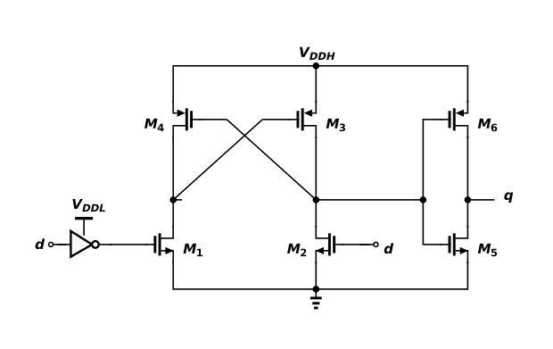
This configuration has three limitations.
1. Unknown power-up state: Even though this level shifter responds to changes in input as required, the power -up state of this level shifter is unknown. During the power-up, q can be either ‘LOW’ or ‘HIGH’. It’s often required for a level shifter to power up in a desired state, either to prevent high currents during power-up or to power up the circuit in a specific configuration.
2. Contention between PMOS and NMOS devices: Whenever ‘d’ transitions from ‘LOW’ to ‘HIGH’, there is contention between M3 and M2. Similar contention exists between M1 and M4, during the opposite transition of ‘d’. This contention will increase the delay of the level shifter as well as its power consumption.
3. Weak drive of input devices: Since M1 and M2 are controlled by signals with ‘VDDL’ swing, they need to be sized significantly larger than M3 and M4 transistors.
Level shifter with known powerup state
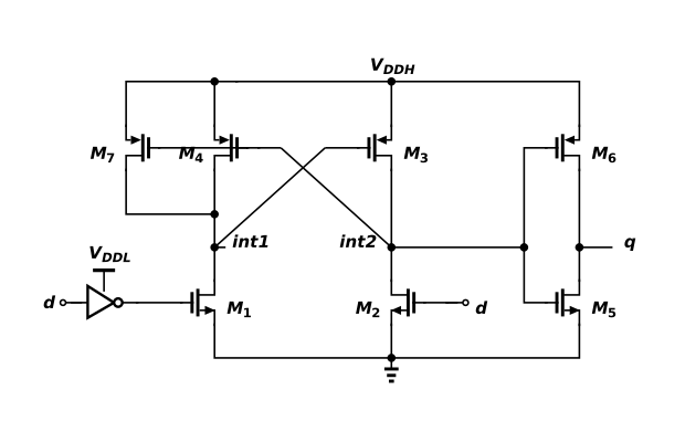
If a level shifter is made asymmetrical, it can force level shifter to powerup in a known, desirable state. For example, the level shifter below had asymmetrical PMOS sizes. During powerup, since M4 and M7 together are stronger than M3, the ‘int1’ net gets charged at faster rate compared to int2 net. This will make level shifter ‘q’ into a ‘HIGH’ state upon powerup.
Level shifter with reduced contention between PMOS and NMOS
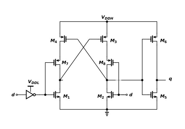
This modified level shifter has two additional PMOS transistors (M7 and M8) compared to previously discussed level shifters. The contention is reduced in this configuration because during d transition from LOW to HIGH, even though M1 and M3 are ON, M8 will be OFF.
Speeding up level shifter further
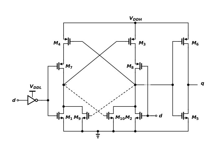
While the previously discussed level shifter improves speed by avoiding contention, performance can be increased further by adding cross-coupled NMOS transistors -M9/M10. Because cross coupled pair (M9/M10), driven by VDDH-domain signals, assists the M1/M2 (driven by VDDL domain signal) in discharging internal nodes, circuit can operate reliably at lower VDDL values.
References
A. Shapiro and E. G. Friedman, “Power Efficient Level Shifter for 16 nm FinFET Near Threshold Circuits,” in IEEE Transactions on Very Large Scale Integration (VLSI) Systems, vol. 24, no. 2, pp. 774-778, Feb. 2016, doi: 10.1109/TVLSI.2015.2409051.